
World Wide Welfare:
high BRIGHTness
semiconductor lasER for
gEneric Use
high BRIGHTness
semiconductor lasER for
gEneric Use
Partner 19 - University of Kassel
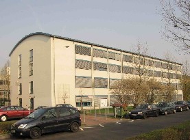
The group at University of Kassel is within the Institute of Nanostructure Technologies and Analytics (INA), originally founded in 1997 as the Institute of Microstructure Technologies and Analytics (IMA) and renamed in 2005.
The institute is a joint laboratory between the physics and electrical engineering departments. The groups within the institute are investigating new micro- and nano-fabrication techniques, device structures and concepts based on III-V and Si technologies.
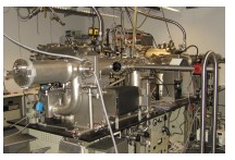
The institute has about 400m2 of clean rooms (class 1000 to class 1) and another 400m2 of laboratory space with an extensive infrastructure, which includes three MBE systems for III-V materials, patterning by optical and e-beam lithography, semiconductor processing (etching, deposition, evaporation) and a range of characterisation tools (AFM, STM, SEM, X-Ray, ellipsometry, etc.).
Within the INA, the technological physics group has been headed by Johann Peter Reithmaier since 2005. Previously he worked at the University of Würzburg, where he was responsible for a research group investigating new nanostructure technologies and optoelectronic device concepts. During this time, the research group developed quantum dot (QD) laser materials and devices for different wavelength ranges (1.0, 1.3, 1.5-2.0 µm).
By tailoring the gain function with the dot dimensions, the group were able, for the first time, to stabilise the emission wavelength of QD lasers, making coolerless high-power pump modules for fibre amplifiers and lasers a possibility. The former group at Würzburg also realised ultra-short edge-emitting QD lasers with deeply etched Bragg mirrors (world record of 12 µm long lasers and 1 mA threshold current with 1 mW cw output power for a 30 µm cavity length).
The group also achieved a record high direct modulation bandwidth of 37 GHz for InP-based 1.5 µm lasers by introducing the concept of a coupled cavity injection grating, which utilises coupling into higher order photonic cavity resonances and improves the limitations caused by the electron-photon coupling by factor of more than 4. Focused ion beam technologies were used to develop highly reliable grating fabrication methods, which allow maskless patterning of 1st order gratings for InP-based DFB lasers.
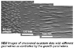
The new group in Kassel is continuing the activities on QD material development based on the self-organization of III-V QDs. The work is being extended to new fabrication technologies, which combine the high resolution and positioning control of state-of-the-art electron beam patterning with defect-free growth techniques to overcome current restrictions in the geometry control of nano-structures.
A major interest is also looking to utilise this new class of material in device applications, (single photon sources, high-speed optoelectronic devices and high-power lasers). For this approach, one MBE system is dedicated to GaAs and one to InP-based materials, allowing wavelength coverage from the visible down to the near infrared. Two additional groups are working on the fabrication and investigation of nanocrystalline diamond and on silicon-based cantilever techniques for sensors.
The former research group in Würzburg was active in several EC projects including: BIGBAND, NANOLASE, NANOPT, ULTRABRIGHT and WWW.BRIGHT.EU. Currently the group in Kassel is involved in four European projects (Pronano, QPhoton, Tasnano and WWW.BRIGHTER.EU)
Activities within WWW.BRIGHT-EU
Within the project, the University of Kassel is realising QD laser structures at 920 nm with tailored QD geometries for coolerless pump laser applications as well as 920 nm and 1060 nm high-performance next generation QD laser material optimised for high wall-plug efficiency, high temperature stability and ultra-low alpha factors for high-brightness tapered lasers with an improved filamentation threshold.
The aim of this approach is to explore the possibility of overcoming single mode output power limitations of conventional QW based technologies by using nanostructured laser material. While the 920 nm laser material will be used for pumping fibre lasers, the 1060 nm material is for devices that will be frequency-doubled to achieve green lasers for display applications.
Further Information
Further information can be obtained from:
Prof. Johann Peter Reithmaier
Tel: +49 561 804 4430
Email: jpreith@physik.uni-kassel.de
Web: http://www.ina.uni-kassel.de
Further information can be obtained from:
Prof. Johann Peter Reithmaier
Tel: +49 561 804 4430
Email: jpreith@physik.uni-kassel.de
Web: http://www.ina.uni-kassel.de


[Home] [Project] [Participants] [Newsletters] [Publications] [Workshops] [Tutorials] [More...] [Private] [Legal notice]
