

World Wide Welfare:
high BRIGHTness
semiconductor lasER for
gEneric Use
high BRIGHTness
semiconductor lasER for
gEneric Use
Partner 16 - (FBH)
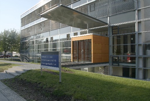
Ferdinand-Braun-Institut für Höchstfrequenztechnik
Ferdinand-Braun-Institut für Höchstfrequenztechnik
The Ferdinand-Braun-Institut explores cutting-edge technologies in the fields of microwaves and optoelectronics based on compound semiconductors. It develops high-frequency devices and circuits for communication and sensor technology. High-power diode lasers with excellent beam quality are produced for materials processing, laser technology, medical technology and high precision metrology.
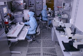
The FBH is an internationally recognized competence centre for III/V-compound semiconductors. It operates industry-compatible and flexible clean room laboratories with equipment for epitaxial layer growth, different III/V-semiconductor process lines and an advanced mounting technology.
The work relies on comprehensive materials and process analysis equipment, a state-of-the-art device measurement environment, and excellent tools for simulation and CAD.
The FBH develops high-value products and services for its partners in the research community and industry which are tailored precisely to fit individual needs. The institute offers complete solutions and know-how as a one-stop agency from design to ready-to-ship modules. The FBH also succeeds in turning innovative product ideas into spin-off companies.
Activities in WWW.BRIGHT-EU
- Within the project the following topics were investigated:
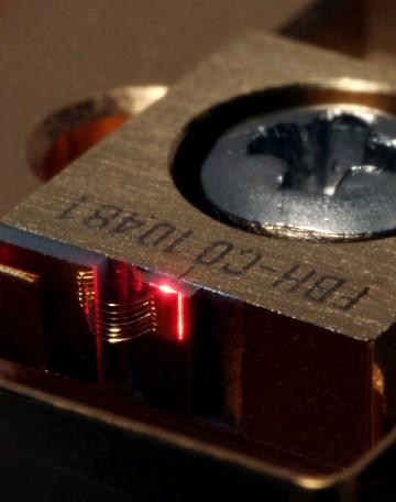
- High-power broad area lasers and bars for medical applications at 652 nm
The manufacturing of high power diode laser devices emitting in the red spectral range is very challenging due to some drawbacks of the laser material like low barriers heights for carriers and low thermal and electrical conductivity.
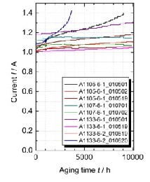
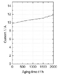
Research work is concentrated on layer design, growth procedure, device processing and mounting. As a result reliable operation were demonstrated over 10000 h at 500 mW output power for 100µm broad area lasers and 2000 h at 5 W for 5mm laser bars.
These values exceed the lifetime demands for laser devices used in medicine (typically 1000 h). Now 100 µm wide broad area lasers with a maximum output power of 3 W and 5 mm bars with 12 W could be realized. The data represent record high output powers for devices at 652 nm. Reliability tests at higher output powers are started.
The results open perspectives for future projects including applications in display technology also.
- Tapered laser devices for the application in external cavities
The use of external cavities to improve the brilliance of high power diode lasers is a common technique to open up new applications. The efficiency of feedback from external mirror or gratings depends strongly on divergence of the diode laser used as gain media.
Within the project 810 nm tapered gain media with very small vertical divergence QFA » 18° (FWHM) were developed. Typically such structures suffer from quite low efficiency due to a very small optical gain.
The structures designed and realized at the FBH have only a slight decrease in efficiency and combines herewith high output power with low vertical divergence. Using these well-suited devices in external cavity partners achieved more then 2W nearly diffraction limited optical power in a single spectral line.
- Within the project the following topics were investigated:
- High-power broad area lasers and bars for medical applications at 652 nm
The manufacturing of high power diode laser devices emitting in the red spectral range is very challenging due to some drawbacks of the laser material like low barriers heights for carriers and low thermal and electrical conductivity.
Research work is concentrated on layer design, growth procedure, device processing and mounting. As a result reliable operation were demonstrated over 10000 h at 500 mW output power for 100µm broad area lasers and 2000 h at 5 W for 5mm laser bars.
These values exceed the lifetime demands for laser devices used in medicine (typically 1000 h). Now 100 µm wide broad area lasers with a maximum output power of 3 W and 5 mm bars with 12 W could be realized. The data represent record high output powers for devices at 652 nm. Reliability tests at higher output powers are started.
The results open perspectives for future projects including applications in display technology also.
- Tapered laser devices for the application in external cavities
The use of external cavities to improve the brilliance of high power diode lasers is a common technique to open up new applications. The efficiency of feedback from external mirror or gratings depends strongly on divergence of the diode laser used as gain media.
Within the project 810 nm tapered gain media with very small vertical divergence QFA » 18° (FWHM) were developed. Typically such structures suffer from quite low efficiency due to a very small optical gain.
The structures designed and realized at the FBH have only a slight decrease in efficiency and combines herewith high output power with low vertical divergence. Using these well-suited devices in external cavity partners achieved more then 2W nearly diffraction limited optical power in a single spectral line.
Current Research Topics
Microwaves
- Gallium arsenide electronics with heterojunction bipolar transistors: MMICs up to 80 GHz and power amplifiers up to 10 GHz
- Gallium nitride electronics: microwave power transistors up to 10 GHz (power: >> 10 Watt)
Optoelectronics
- High power, highly efficient diode laser and laser bars between 800nm and 1060nm
- High-brightness diode lasers up to 10W single emitters
- Narrow linewidth lasers < 1 MHz
- Hybrid laser systems (compact MOPA systems)
- Non-linear frequency conversion with diode lasers as pump sources
- Semiconductor disc lasers
- Gallium nitride based LEDs and lasers
Technologies and facilities
Comprehensive III-V epitaxy equipment
- Comprehensive III-V epitaxy equipment for homogenous semiconductor layer structures, not only for in-house requirements but also for customer-specific layer structures:
- MOVPE for e.g. laser diodes, Schottky diodes, HBTs
- HVPE and MOVPE for GaN based epitaxy
- characterization in order to optimise processes and development
Complete and industry-compatible process lines
- Complete and industry-compatible process line: consists of all enabling technologies for chip manufacturing from structuring and deposition techniques to chip dicing.
- wafers from 2" to 4"
- different types of substrates: GaAs, InP, Si, SiC, glass and others with high reproducibility
FBH offers complete processes up to small-scale series fabrication or transfers process modules to external partners.
Mounting and packaging
- Mounting and packaging: a key competence for laser diodes as well as for microwave transistors and circuits. For diode lasers:
- Separation of wafers to chips by scribing and breaking
- Soldering of diode lasers and laser bars
- Wire bonding
- Hybrid integration of diode lasers and electronic components
- Active alignment of optical components and diode lasers: beam shaping & hybrid integrated MOPA (Master Oscillator Power Amplifier) systems
[Home] [Project] [Participants] [Newsletters] [Publications] [Workshops] [Tutorials] [More...] [Private] [Legal notice]