

World Wide Welfare:
high BRIGHTness
semiconductor lasER for
gEneric Use
high BRIGHTness
semiconductor lasER for
gEneric Use
Partner 11- University of Würzburg
Overall presentation
Overall presentation
The group at Würzburg University is investigating different III-V material systems and new concepts for the development of opto-electronic devices. Based on high-resolution lithographic systems, nanostructure patterning techniques with minimum feature sizes below 10 nm were developed for opto-electronic applications as well as for basic physics studies.
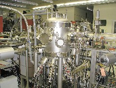
The Microfabrication Laboratory of the group (550 m2 cleanroom) includes solid source and gas source MBE systems for different III-V material systems, high resolution electron beam lithography, a high resolution focused ion beam system, different dry etching systems, cw-, pulsed and high frequency measurement tools for opto-electronic devices. For basic material studies e.g. high-Q cavities high resolution photo-luminescence setups are available.
Also, transport properties of nano-structured electronic devices are investigated. Based on molecular beam epitaxy, low threshold, high efficiency quantum well and quantum dot laser structures were developed for high power and telecommunication applications.
Based on different material systems (GaAs, InP, GaSb), we cover the whole wavelength range from about 0.8 to 2.7 µm. Record values in cw output powers of quantum dot lasers of 6.3 W were achieved at 980 nm.
Quantum dot lasers for 1.3 µm emission wavelengths were realized with high device performance (e.g. Ith = 2 mA for 400 µm long device) and for longer wavelength appli-cations quantum dash structures were developed on InP substrates with transparency current densities < 500 A/cm2 and emission wavelengths in the range between 1.4 to 2 µm.
Ridge waveguide lasers achieved threshold currents below 20 mA at room temperature (300 µm long device).
The first room temperature lasers worldwide emitting > 1.5 µm on GaAs using nitride-containing layers were reported in 2000.
Also research activities on quantum cascade lasers for mid and far infra-red on GaAs and on InP are performed within the group.
By using high-resolution lateral patterning tech-niques (electron and focused ion beam lithography), complex-coupled DFB lasers with first order gratings were developed for telecommunication and sensor applications in different material systems and for different wavelength ranges (0.8 - 1 µm, 1.3 µm, 1.55 µm and > 2 µm).
Devices in the 1.55 µm wavelength range were developed for high speed applications. High frequency operation up to 22 GHz has been achieved on high performance single mode lasers.
New design concepts were developed based on multi-section structures, which allow a strong enhancement of the high frequency properties. Up to 37 GHz small signal modulation bandwidth was demonstrated.
Another major research activity is the fabrication and characterization of photonic crystal structures, which require both high resolution E-beam and dry etching techniques. This approach requires the development of etch processes with high aspect ratios, smooth sidewalls and excellent geometry control.
A number of novel opto-electronic devices (e.g. PC based lasers) as well as structures for fundamental studies of photonic crystals have been realized with this technology.
The major devices and device concepts have been developed within the frame of different national and European projects in cooperation with large industrial partners (e.g. Infineon, Alcatel, Thales ) and different medium and small size companies.
The research group was and is active as coordinator and partner in different EU projects (e.g. NANOPT, NANOLASE, Q-SWITCH, PCIC, ULTRABRIGHT, NANO-TCAD, BIGBAND; FUNFOX, ZODIAC, WWW. BRIGHT-EU, ).
Activities in WWW.BRIGHT-EU
Within the project, the group at Würzburg University is realizing quantum dot laser structures at 915 nm for uncooled pump applications.
The goal is to make use of the improved temperature stability of the emission wavelength of the quantum dots to achieve a thermal induced wavelength shift lower than 0.1 nm/K. From these structures, tapered lasers are processed to investigate the capability of quantum dots in uncooled pump modules.
Another task is the implementation of lateral gratings on tapered lasers for wavelength stabilization and multiplexing.
The aim within this project is to achieve more than 1 W of single mode output power from a 915 nm quantum dot laser.
[Home] [Project] [Participants] [Newsletters] [Publications] [Workshops] [Tutorials] [More...] [Private] [Legal notice]