

World Wide Welfare:
high BRIGHTness
semiconductor lasER for
gEneric Use
high BRIGHTness
semiconductor lasER for
gEneric Use
Partner 1- Alcatel Thales III-V Lab
Overall presentation
Alcatel Thales III-V Lab is a private non-profit organisation jointly established by Alcatel and Thales on 1st July 2004, under the French Economic Interest Group (GIE) status. Relying on the expertise of Alcatel CIT Research and Innovation and Thales Research and Technology, it concentrates in a single entity one of the most advanced industrial research groups in the field of III-V semiconductors in Europe. The staff numbers approximately 100 highly qualified people, most of them recognised experts in their area.
Alcatel Thales III-V Lab performs research on components, from the basic studies to the transfer for industrialisation, by exploiting the synergies between the technologies developed for various markets addressed by Thales and Alcatel, such as telecom, space, defence and security. The streamlining of the research work performed within the Group strengthens these efforts to exceed the critical mass and to increase the added value through the existing synergies.
Alcatel Thales III-V Lab is located in Marcoussis and Orsay and includes 4000 m2 of clean rooms, advanced material synthesis (MOCVD, MBE), advanced material processing (RIE, ICP, CAIBE, IBE), measuring and modelling facilities. Some of the Orsay facilities will move to the new Thales Research and Technology facility in Palaiseau by June 2005.
Main research topics
- Optical sources and detectors for telecom 10-40Gb/s
- Micro/nano-electronics circuits for telecom 40Gb/s (analogue and digital)
- N+2 generation telecom components,
- High data rate optical links
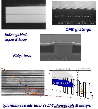
- High power and high brightness semiconductor lasers
- Quantum cascade semiconductor lasers
- Semiconductor lasers for atomic clocks and gas detection
- Quantum dot lasers
- High speed analogue optoelectronic components and functions for microwave photonics
- Microwave components based on GaN (high yield, wide band)
- High-resolution imaging
- Optical sources and detectors for telecom 10-40Gb/s
- Micro/nano-electronics circuits for telecom 40Gb/s (analogue and digital)
- N+2 generation telecom components,
- High data rate optical links
- High power and high brightness semiconductor lasers
- Quantum cascade semiconductor lasers
- Semiconductor lasers for atomic clocks and gas detection
- Quantum dot lasers
- High speed analogue optoelectronic components and functions for microwave photonics
- Microwave components based on GaN (high yield, wide band)
- High-resolution imaging
Technologies and facilities
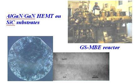
Epitaxial growth of III-V semiconductors
- Multi-wafer MBE, GS-MBE, MO-VPE reactors
- Complex heterostructures based on GaAs, InP, SiC and GaSb substrates
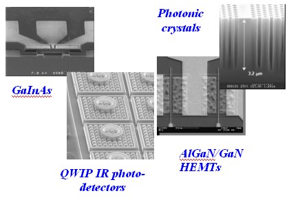
Clean room device processing
- Microelectronic technologies: lithography, metal and dielectric material deposition and etching,
- Microwave and fast digital devices and circuits: InP HBTs, GaN HEMT
- Opto-electronic devices (lasers, modulators, photo-detectors )
Measurement, simulation and design
- Physical modelling of microelectronic and optoelectronic devices
- Linear and non-linear equivalent circuits
- Microwave and fast digital circuit design and simulation
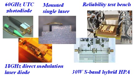
Module and sub-system demonstrators
- Optoelectronic module demonstrators (40Gb/s transceivers )
- Microwave amplifiers demonstrators
- Operational reliability evaluations
Epitaxial growth of III-V semiconductors
- Multi-wafer MBE, GS-MBE, MO-VPE reactors
- Complex heterostructures based on GaAs, InP, SiC and GaSb substrates
Clean room device processing
- Microelectronic technologies: lithography, metal and dielectric material deposition and etching,
- Microwave and fast digital devices and circuits: InP HBTs, GaN HEMT
- Opto-electronic devices (lasers, modulators, photo-detectors )
Measurement, simulation and design
- Physical modelling of microelectronic and optoelectronic devices
- Linear and non-linear equivalent circuits
- Microwave and fast digital circuit design and simulation
Module and sub-system demonstrators
- Optoelectronic module demonstrators (40Gb/s transceivers )
- Microwave amplifiers demonstrators
- Operational reliability evaluations
[Home] [Project] [Participants] [Newsletters] [Publications] [Workshops] [Tutorials] [More...] [Private] [Legal notice]